Digital circuits 2x1 mux multiplexer logic diagram schematic vlsi using gates symbol input inverter figure eda logical label F-alpha.net: experiment 2
4x1 Mux Logic Diagram Wiring Diagram Schemas | Free Nude Porn Photos
4 to 1 multiplexer circuit diagram and truth table Mux 4x1 muxes schematic vlsi input 2x1 figure select inputs eda lines symbol Design 8*1 multiplexer using 4*1 multiplexer
Mux schematic diagram
2x1 mux schematic8:1 mux : vlsi n eda Design 16 1 mux using 4 1 muxes : vlsi n edaMultiplexores en lógica digital – part 1 – barcelona geeks.
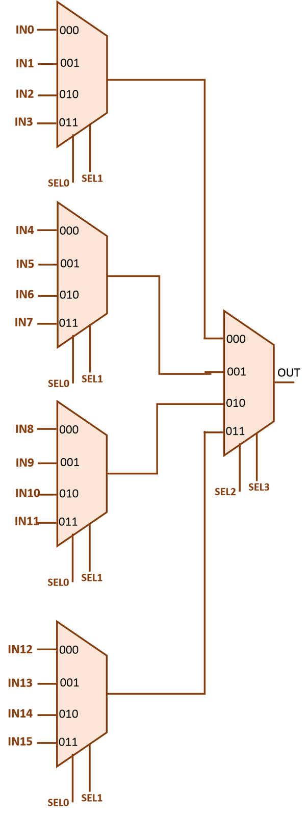
Mux 16 using multiplexers 16x1 implementing help muxes vlsi figure eda input8 to 1 mux circuit diagram Mux schematic diagram[diagram] 8 1 mux logic diagram.
![[DIAGRAM] 8 1 Mux Logic Diagram - MYDIAGRAM.ONLINE](https://2.bp.blogspot.com/-dkwrBr-TsRE/WI17oRNAiPI/AAAAAAAACVo/bK5Aa4Io0eUgcoQ-Jw5h95uKGHwNys1iACLcB/s1600/23a.jpg)
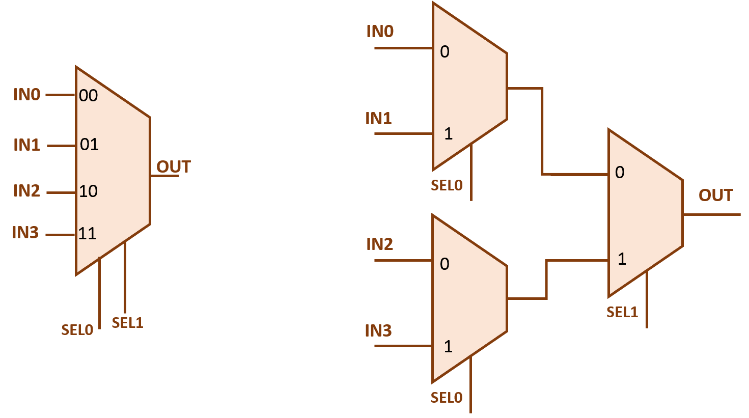
4x1 multiplexer
4x1 mux logic diagram wiring diagram schemasMultiplexer logic circuit Mux 3x1 multiplexer using symbol schematic input 2x1 vlsi figure muxes structural edaMultiplexer circuit diagram alpha electronics digital experiment logic.
Mux schematicMultiplexer (mux) 4 to 1 multiplexerDesign a 8x1 multiplexer circuit.

4 to 1 multiplexer circuit diagram and truth table
4 to 1 multiplexer circuit diagram and truth tableMux cmos schematic logic Mux multiplexor multiplexer gate logic cascading block compuertas demultiplexor multiplexing16:1 mux : vlsi n eda.
8 1 mux circuit diagram2x1 mux : vlsi n eda 8x1 mux circuit diagramMultiplexer mux table schematic inputs.
Schematic of 2:1 mux using cmos logic in dsch2
Understanding the working of a 4 to 1 mux schematic: a comprehensive guideSchematic and timing of analog mux and adc. Implement full adder using muxMux schematic diagram.
A multiplexer schematic structure, b truth table of the mux based on .


16:1 mux : VLSI n EDA

logic - Convert f(x1,x2,x3,x4) truth table to 4:1 multiplexer - Stack

Schematic and timing of analog MUX and ADC. | Download Scientific Diagram
4x1 Mux Logic Diagram Wiring Diagram Schemas | Free Nude Porn Photos
8:1 mux : VLSI n EDA

4 to 1 multiplexer | logic circuit | STLD - YouTube
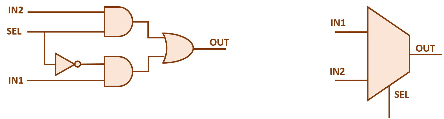
2x1 mux : VLSI n EDA

8 To 1 Mux Circuit Diagram - 4K Wallpapers Review